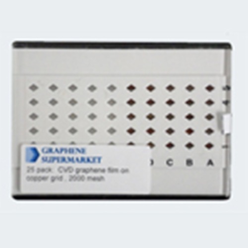
25 pack: CVD Graphene film deposited on ultrafine copper TEM grids, 2000 Mesh
Availability: Out of Stock
Lead time: 4 to 6 weeks
We use CVD graphene grown on Ni to prepare TEM grids
Thickness of CVD Graphene film: 0.3-2 nm (1-6 monolayers)
Typical graphene coverage:60-90%
Ultrathin CVD Graphene grids provide the ideal specimen support to achieve high resolution data in TEM imaging making them an ideal choice many TEM applications such as:
CVD Graphene grids can be used for the applications:
• Imaging of nanoparticles, proteins, viruses, DNA
• Medical Diagnostics
• Single Cell Studies
• 3D protein imaging
• Drug design
• Imaging of Biological Markers and bio-inspired nanomaterials
• Cryo-transmission electron microscopy, Electron Cryomicroscopy
• Single Particle Analysis ( SPA )
• Materials science and Semiconductor Research
• Electron Energy Loss Spectroscopy (EELS)
![]()
| |
| SKU | SKU-TEM-CU-2000-025 |
| Weight | 0.10 lbs |
Customers who bought this product also bought