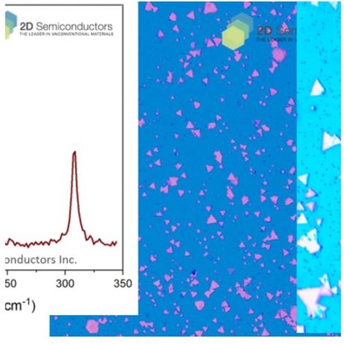
Chemical vapor deposited (CVD) GaSe films have been synthesized at our facilities in 2019. Bulk GaSe is a 2.0 eV direct semiconductor with exciting second harmonic, optical, and photovoltaics applications. It crystallizes in hexagonal structure. CVD GaSe samples measure nearly 1x1cm2 in size. The sample does not reach full continuity instead one can find many isolated GaSe triangles that measure 1L to 100s of layer in thickness. By default it is grown onto SiO2/Si or (100) GaAs substrates.
The characteristics of CVD GaSe
| Sample size | 1cm x 1cm might have uneven sample shape |
| Substrate type | SiO2/Si or GaAs |
| Coverage | Isolated triangles |
| Electrical properties | Direct gap semiconductor (bulk) indirect gap semiconductor (monolayer) |
| Crystal structure | Hexagonal phase |
| Unit cell parameters | a=b=0.376 nm, c=1.596 nm, α=β=90°, γ=120° |
| Production method | Chemical vapor deposition |
| Characterization methods | Raman, photoluminescence, TEM, EDS |
상품의 사용후기를 적어주세요.
게시물이 없습니다
상품에 대해 궁금한 점을 해결해 드립니다.
게시물이 없습니다


법인명(상호) : 유니나노텍(주) 대표자(성명) : 유니나노텍(주) 사업자 등록번호 안내 : [1428150860] 통신판매업 신고 2021-용인기흥-0779 [사업자정보확인]
전화 : 031-546-8733 팩스 : 주소 : 17015 경기도 용인시 기흥구 동백중앙로16번길 16-4 (중동) 에이스동백타워 1동 303호
개인정보보호책임자 : 유니나노텍(주)(nano@uninanotech.com)
Contact for more information.
Copyright © 유니나노텍(주). All rights reserved. hosting by cafe24 카페24(주)