| 상품명 | Few layer Full Area Coverage MoSe2 |
|---|---|
| 상품요약정보 | Few layer Full Area Coverage MoSe2 |
| 국내·해외배송 | 국내배송 |
| 배송방법 | 택배 |
| 배송비 | 2,500원 (50,000원 이상 구매 시 무료) |
| SNS 상품홍보 | |
|---|
배송주기

| 옵션선택 |
(최소주문수량 1개 이상 / 최대주문수량 0개 이하)
사이즈 가이드수량을 선택해주세요.
위 옵션선택 박스를 선택하시면 아래에 상품이 추가됩니다.
| 상품명 | 상품수 | 가격 |
|---|---|---|
| Few layer Full Area Coverage MoSe2 |


|
0 ( |
할인가가 적용된 최종 결제예정금액은 주문 시 확인할 수 있습니다.
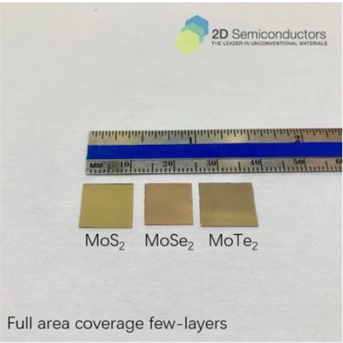
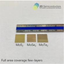
This product contains full area coverage MoSe2 few-layers that measure ~5 layers in thickness. Sheets are grown through chemical vapor deposition technique onto c-cut double side polished sapphire substrates, but layers can be transferred onto other substrates by polymer assisted transfer technique on demand (please select from the drop down menu). The sample measures 1cm2 in size and the entire sample surface contains few-layer thick MoSe2 sheet. Grown few-layers are high-crystalline as evidenced by HR-TEM, Raman, EDS, and XRD measurements.
Our company synthesizes these few layers using chemical vapor deposition (CVD) with highest purity (6N) gases and precursors in semiconductor grade facilities. This produces highly crystalline and large domain size samples that range from 1 to 50 microns in lateral sizes. CVD grown samples from other sources typically use MOCVD or sputtering process wherein carbon contamination is problematic, defect density is extremely large, domain sizes are small (10nm-500nm). Our samples are always highly crystallized, high purity, and perfectly layered.
Sample Properties
| Sample size | 1cm x 1cm square shaped |
| Substrate type | Substrate of your choice |
| Coverage | Full Coverage few layers |
| Electrical properties | Indirect gap semiconductor |
| Crystal structure | Hexagonal Phase |
| Unit cell parameters | a = b = 0.33 nm, c = 1.292 nm, α = β = 90°, γ = 120° |
| Production method | Chemical Vapor Deposition (CVD) |
| Characterization methods | Raman, photoluminescence, TEM, EDS |
상품의 사용후기를 적어주세요.
게시물이 없습니다
상품에 대해 궁금한 점을 해결해 드립니다.
게시물이 없습니다


법인명(상호) : 유니나노텍(주) 대표자(성명) : 유니나노텍(주) 사업자 등록번호 안내 : [1428150860] 통신판매업 신고 2021-용인기흥-0779 [사업자정보확인]
전화 : 031-546-8733 팩스 : 주소 : 17015 경기도 용인시 기흥구 동백중앙로16번길 16-4 (중동) 에이스동백타워 1동 303호
개인정보보호책임자 : 유니나노텍(주)(nano@uninanotech.com)
Contact for more information.
Copyright © 유니나노텍(주). All rights reserved. hosting by cafe24 카페24(주)