| 상품명 | Graphene on Cu foils |
|---|---|
| 상품요약정보 | Graphene on Cu foils |
| 국내·해외배송 | 국내배송 |
| 배송방법 | 택배 |
| 배송비 | 2,500원 (50,000원 이상 구매 시 무료) |
| SNS 상품홍보 | |
|---|
배송주기

| 옵션선택 |
(최소주문수량 1개 이상 / 최대주문수량 0개 이하)
사이즈 가이드수량을 선택해주세요.
위 옵션선택 박스를 선택하시면 아래에 상품이 추가됩니다.
| 상품명 | 상품수 | 가격 |
|---|---|---|
| Graphene on Cu foils |


|
0 ( |
할인가가 적용된 최종 결제예정금액은 주문 시 확인할 수 있습니다.
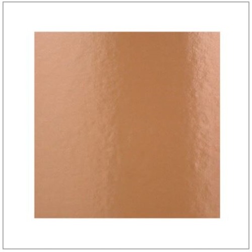
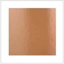
CVD Graphene sheets have been deposited onto 50 micron thick Cu foils using modified chemical vapor technique. In our method, we have paid close attention to engineering defect density and single domain sizes. Most CVD graphene chambers produce small (100nm - 1um) graphene sheets. Our process parameters have been optimized to reduce the point defect (vacancy) concentration, improve crystallinity, increase single domain size, and reduce 1D grain boundary defect density. Our CVD graphene products undergo weekly routine quality control tests to ensure the growth system is accurate and parameters are up to date. Our CVD graphene on copper foils measure 2 inches x 2 inches (~5 x5 cm in size).
If your research needs graphene transferred onto other substrates (SiO2/Si, TEM grids, PET, and other), please contact us for competitive pricing options.
Advantages of CVD graphene on copper foils from 2Dsemiconductors USA
Properties of graphene on copper
Raman spectrum on CVD graphene on copper (2x2 inches)
TEM images collected from CVD graphene transferred onto TEM grids
SEM image collected from graphene/copper surfaces
상품의 사용후기를 적어주세요.
게시물이 없습니다
상품에 대해 궁금한 점을 해결해 드립니다.
게시물이 없습니다


법인명(상호) : 유니나노텍(주) 대표자(성명) : 유니나노텍(주) 사업자 등록번호 안내 : [1428150860] 통신판매업 신고 2021-용인기흥-0779 [사업자정보확인]
전화 : 031-546-8733 팩스 : 주소 : 17015 경기도 용인시 기흥구 동백중앙로16번길 16-4 (중동) 에이스동백타워 1동 303호
개인정보보호책임자 : 유니나노텍(주)(nano@uninanotech.com)
Contact for more information.
Copyright © 유니나노텍(주). All rights reserved. hosting by cafe24 카페24(주)