| 상품명 | Hexagonal Boron Nitride (h-BN, BN2A1) |
|---|---|
| 상품요약정보 | Hexagonal Boron Nitride (h-BN, BN2A1) |
| 국내·해외배송 | 국내배송 |
| 배송방법 | 택배 |
| 배송비 | 2,500원 (50,000원 이상 구매 시 무료) |
| SNS 상품홍보 | |
|---|
배송주기

| 옵션선택 |
(최소주문수량 1개 이상 / 최대주문수량 0개 이하)
사이즈 가이드수량을 선택해주세요.
위 옵션선택 박스를 선택하시면 아래에 상품이 추가됩니다.
| 상품명 | 상품수 | 가격 |
|---|---|---|
| Hexagonal Boron Nitride (h-BN, BN2A1) |


|
0 ( |
할인가가 적용된 최종 결제예정금액은 주문 시 확인할 수 있습니다.
Hexagonal boron nitride is a semiconductor with a direct band gap of ~5.9 eV and has been used extensively as an insulator for the production of ultrahigh mobility 2D heterostructures composed of various types of 2D semiconductors (e.g. WSe2, MoSe2, etc). The layers are stacked together via van der Waals interactions and can be exfoliated into thin 2D layers, down to monolayer h-BN. To buy hexagonal boron nitride crystals please click here.
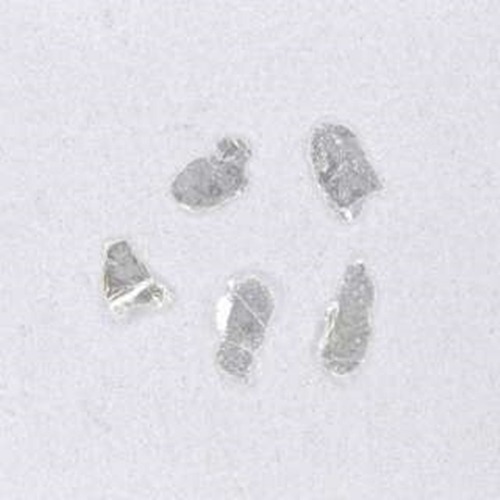
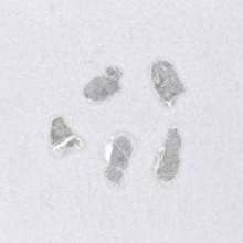
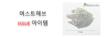
The h-BN crystals from HQ Graphene have a typical lateral size of ~0.1 cm and are transparent. The monocrystalline h-BN is an excellent insulator which is represented by its very large breakdown voltage (>0.4 V/nm). Large area size h-BN single crystals can be can be exfoliated onto a substrate (eg. SiO2, quartz, polymer, etc). Sizes range up to ~100 μm for crystals with a thickness of a few tens on nm thick. A selection of peer review publications on the hexagonal Boron Nitride we sell can be found below.
| Crystal size | ~1 mm |
| Electrical properties | Insulator/Semiconductor |
| Crystal structure | Hexagonal |
| Unit cell parameters | a = b = 0.2502 nm, c = 0.6617 nm, α = β = 90°, γ = 120° |
| Type | Synthetic |
| Purity | Grade A |
| Characterized by | XRD, Raman, EDX |
| More information? | Please contact us by email or phone |
XRD: single crystal and powder X-ray diffraction (D8 Venture Bruker and D8 Advance Bruker)
EDX: Energy-dispersive X-ray spectroscopy for stoichiometric analysis
Raman: 785nm Raman system
Click on an image to zoom
X-ray diffraction on a hexagonal boron nitride single crystal aligned along the (001) plane. XRD was performed at room temperature using a D8 Venture Bruker. The 4 XRD peaks correspond, from left to right, to (00l) with l = 1, 2, 3
Raman spectrum of a single crystal hexagonal boron nitride (h-BN). Measurement was performed with a 785nm Raman system at room temperature.
Device at left side: Fabrication of a high mobiltity bilayer graphene. This field effect transistor is fabricated using the polymer 2D_CL_PC ( click here ). The device is composed out of four 2D layers. The bilayer graphene is encapsulated between two hexagonal boron nitride crystals (h-BN). The fourth layer is a thin layer of graphite (HOPG) which is used as a backgate. Scale bar is 20μm. Device at right side: This device is similar to the one at the left side, here we added on the top hexagonal boron nitride layer a gold electrode in order to apply a top gate voltage to the hBN encapsulated bilayer graphene. Scale bar is 20μm
1. G. Cassabois et al., "Hexagonal boron nitride is an indirect bandgap semiconductor", Nature photonics 10, 262-266 (2016), link to article:http://www.nature.com/nphoton/journal/v10/n4/full/nphoton.2015.277.html
2. S. Dufferwiel et al. "Exciton-polaritons in van der Waals heterostructures embedded in tunable microcavities", Nature Communications 6, 8579 (2015), link to article:http://www.nature.com/articles/ncomms9579?WT.ec_id=NCOMMS-20151010
상품의 사용후기를 적어주세요.
게시물이 없습니다
상품에 대해 궁금한 점을 해결해 드립니다.
게시물이 없습니다


법인명(상호) : 유니나노텍(주) 대표자(성명) : 유니나노텍(주) 사업자 등록번호 안내 : [1428150860] 통신판매업 신고 2021-용인기흥-0779 [사업자정보확인]
전화 : 031-546-8733 팩스 : 주소 : 17015 경기도 용인시 기흥구 동백중앙로16번길 16-4 (중동) 에이스동백타워 1동 303호
개인정보보호책임자 : 유니나노텍(주)(nano@uninanotech.com)
Contact for more information.
Copyright © 유니나노텍(주). All rights reserved. hosting by cafe24 카페24(주)