| 상품명 | Molybdenum Ditelluride (2H MoTe₂) |
|---|---|
| 상품요약정보 | Molybdenum Ditelluride (2H MoTe₂) |
| 국내·해외배송 | 국내배송 |
| 배송방법 | 택배 |
| 배송비 | 2,500원 (50,000원 이상 구매 시 무료) |
| SNS 상품홍보 | |
|---|
배송주기

| 옵션선택 |
(최소주문수량 1개 이상 / 최대주문수량 0개 이하)
사이즈 가이드수량을 선택해주세요.
위 옵션선택 박스를 선택하시면 아래에 상품이 추가됩니다.
| 상품명 | 상품수 | 가격 |
|---|---|---|
| Molybdenum Ditelluride (2H MoTe₂) |


|
0 ( |
할인가가 적용된 최종 결제예정금액은 주문 시 확인할 수 있습니다.
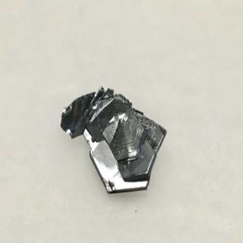
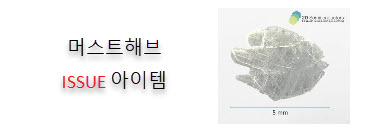
2H semiconducting phase of MoTe2 crystals contain layers that are stacked together via van der Waals interactions and can be exfoliated into thin 2D layers. Our large size 2H-MoTe2 vdW crystals are treated as gold standards in 2D materials field. They come with guaranteed valleytronic performance, clean PL spectrum, perfect crystallization, and defect free structure. Our MoTe2 crystals are synthesized two different methods (flux zone and chemical vapor transport). While flux zone provides extremely clean MoTe2 crystals, CVT method often introduces halide contaminants. For comparison between these tow methods, please see the information below. If your research needs electronically doped MoTe2 crystals, please contact us.
Characteristics of 2H-MoTe2 crystals from 2Dsemiconductors USA
Growth method matters> Flux zone or CVT growth method? Contamination of halides and point defects in layered crystals are well known cause for their reduced electronic mobility, reduced anisotropic response, poor e-h recombination, low-PL emission, and lower optical absorption. Flux zone technique is a halide free technique used for synthesizing truly semiconductor grade vdW crystals. This method distinguishes itself from chemical vapor transport (CVT) technique in the following regard: CVT is a quick (~2 weeks) growth method but exhibits poor crystalline quality and the defect concentration reaches to 1E11 to 1E12 cm-2 range. In contrast, flux method takes long (~3 months) growth time, but ensures slow crystallization for perfect atomic structuring, and impurity free crystal growth with defect concentration as low as 1E9 - 1E10 cm-2. During check out just state which type of growth process is preferred. Unless otherwise stated, 2Dsemiconductors ships Flux zone crystals as a default choice.
Y. Li et. al. "Room-temperature continuous-wave lasing from monolayer molybdenum ditelluride integrated with a silicon nanobeam cavity"
Nature Nanotechnology volume 12, pages 987–992 (2017)
Control of Exciton Valley Coherence in Transition Metal Dichalcogenide Monolayers, Phys. Rev. Lett. 117, 187401 (2016)
Tony Heinz Team "Optical Properties and Band Gap of Single- and Few-Layer MoTe2 Crystals" Nano Letters 2014, 14, 6231−6236
Physical origin of Davydov splitting and resonant Raman spectroscopy of Davydov components in multilayer MoTe2; Q. J. Song, Q. H. Tan, X. Zhang, J. B. Wu, B. W. Sheng, Y. Wan, X. Q. Wang, L. Dai, and P. H. Tan; Phys. Rev. B 93, 115409 (2016)
Indirect-to-Direct Band Gap Crossover in Few-Layer MoTe2; Ignacio Gutiérrez Lezama et. al. Nano Letters 2015, 15 (4), pp 2336–2342 DOI: 10.1021/nl5045007
Measurement of the optical dielectric function of monolayer transition-metal dichalcogenides: MoS2, MoSe2, WS2, and WSe2, Yilei Li, Alexey Chernikov, Xian Zhang, Albert Rigosi, Heather M. Hill, Arend M. van der Zande, Daniel A. Chenet, En-Min Shih, James Hone, and Tony F. Heinz; Phys. Rev. B 90, 205422 (2014)
M. Yankowitz et. al. "Intrinsic Disorder in Graphene on Transition Metal Dichalcogenide Heterostructures" Nano Letters, 2015, 15 (3), pp 1925–1929
H. C. Diaz et.al. "Molecular beam epitaxy of the van der Waals heterostructure MoTe2 on MoS2: phase, thermal, and chemical stability" 2D Materials, Volume 2, Number 4 (2015)
S. Vishwanath et. al. "MBE growth of few-layer 2H-MoTe2 on 3D substrates" Journal of Crystal Growth, 482, Pages 61-69 (2018)
상품의 사용후기를 적어주세요.
게시물이 없습니다
상품에 대해 궁금한 점을 해결해 드립니다.
게시물이 없습니다


법인명(상호) : 유니나노텍(주) 대표자(성명) : 유니나노텍(주) 사업자 등록번호 안내 : [1428150860] 통신판매업 신고 2021-용인기흥-0779 [사업자정보확인]
전화 : 031-546-8733 팩스 : 주소 : 17015 경기도 용인시 기흥구 동백중앙로16번길 16-4 (중동) 에이스동백타워 1동 303호
개인정보보호책임자 : 유니나노텍(주)(nano@uninanotech.com)
Contact for more information.
Copyright © 유니나노텍(주). All rights reserved. hosting by cafe24 카페24(주)