
| 상품명 | Molybdenum Tungsten Diselenide (MoWSe₂) |
|---|---|
| 상품요약정보 | Molybdenum Tungsten Diselenide (MoWSe₂) |
| 국내·해외배송 | 국내배송 |
| 배송방법 | 택배 |
| 배송비 | 2,500원 (50,000원 이상 구매 시 무료) |
| SNS 상품홍보 | |
|---|
배송주기

| 옵션선택 |
(최소주문수량 1개 이상 / 최대주문수량 0개 이하)
사이즈 가이드수량을 선택해주세요.
위 옵션선택 박스를 선택하시면 아래에 상품이 추가됩니다.
| 상품명 | 상품수 | 가격 |
|---|---|---|
| Molybdenum Tungsten Diselenide (MoWSe₂) |


|
0 ( |
할인가가 적용된 최종 결제예정금액은 주문 시 확인할 수 있습니다.
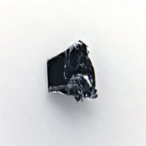
Our MoWSe2 alloys with the chemical formula MoxW(1-x)Se2 crystals perfectly crystallize in 2H phase and come at different alloy ratios x. Our crystals are grown using two different techniques through chemical vapor transport (CVT) or flux zone growth (see description of these two methods below) and their composition values were determined by XPS, SAED, and EDS measurements.. These crystals all possess extremely narrow PL bandwidths, display clean PL spectra, high carrier mobility, extremely clean and sharp XRD peaks, and negligible amount of defects (see published results as well as CVT vs. Flux based methods below ). These crystals come with guaranteed alloying and valleytronic response, sharp PL, and good electronic response.
Important advantages of our crystals
1. Crystals come fully characterized using macro, micro, and nanoscale measurements (see below)
2. Thanks to our improved flux zone growth method, our crystals are homogeneously alloyed which means across the specimen you will only find one particular x composition.
3. No separation: Phase separation is commonly observed in 2D TMDCs alloys when cooling profiles are not controlled carefully. Our R&D team has worked over five (5) years to solely solve this problem.
Properties of layered MoWSe2 alloys
Growth method matters> Flux zone or CVT growth method? Contamination of halides and point defects in layered crystals are well known cause for their reduced electronic mobility, reduced anisotropic response, poor e-h recombination, low-PL emission, and lower optical absorption. Flux zone technique is a halide free technique used for synthesizing truly semiconductor grade vdW crystals. This method distinguishes itself from chemical vapor transport (CVT) technique in the following regard: CVT is a quick (~2 weeks) growth method but exhibits poor crystalline quality and the defect concentration reaches to 1E11 to 1E12 cm-2 range. In contrast, flux method takes long (~3 months) growth time, but ensures slow crystallization for perfect atomic structuring, and impurity free crystal growth with defect concentration as low as 1E9 - 1E10 cm-2. During check out just state which type of growth process is preferred. Unless otherwise stated, 2Dsemiconductors ships Flux zone crystals as a default choice.
http://meetings.aps.org/Meeting/MAR18/Session/K36.3
http://meetings.aps.org/Meeting/MAR17/Session/V1.14
Raman datasets collected from MoWSe2 alloys
Photoluminescence specturm collected from MoWSe2 alloys at 300K
Publications from this product
Summary: Publications from MIT, Berkeley, Stanford, Rice, and Harvard teams at top journals like Nature, Nature Communications, Nano Letters, and Advanced Materials
Control of Exciton Valley Coherence in Transition Metal Dichalcogenide Monolayers, Phys. Rev. Lett. 117, 187401 (2016)
Measurement of the optical dielectric function of monolayer transition-metal dichalcogenides: MoS2, MoSe2, WS2, and WSe2, Yilei Li, Alexey Chernikov, Xian Zhang, Albert Rigosi, Heather M. Hill, Arend M. van der Zande, Daniel A. Chenet, En-Min Shih, James Hone, and Tony F. Heinz; Phys. Rev. B 90, 205422 (2014)
Y. Jin "A Van Der Waals Homojunction: Ideal p–n Diode Behavior in MoSe2" Advanced Materials 27, 5534–5540 (2015)
Tongay et. al. "Defects activated photoluminescence in two-dimensional semiconductors: interplay between bound, charged, and free excitons" Scientific Reports 3, Article number: 2657 (2013)
M. Yankowitz et. al. "Intrinsic Disorder in Graphene on Transition Metal Dichalcogenide Heterostructures" Nano Letters, 2015, 15 (3), pp 1925–1929
Tongay et.al. Thermally Driven Crossover from Indirect toward Direct Bandgap in 2D Semiconductors: MoSe2 versus MoS2; Nano Letters, 2012, 12 (11), pp 5576–5580
Manish Chhowalla, "Two-dimensional semiconductors for transistors" Nature Reviews Materials 1, Article number: 16052 (2016) doi:10.1038/natrevmats.2016.52
X Li et al. "Determining layer number of twodimensional flakes of transition-metal dichalcogenides by the Raman intensity from substrates" Nanotechnology 27 (2016) 145704
상품의 사용후기를 적어주세요.
게시물이 없습니다
상품에 대해 궁금한 점을 해결해 드립니다.
게시물이 없습니다


법인명(상호) : 유니나노텍(주) 대표자(성명) : 유니나노텍(주) 사업자 등록번호 안내 : [1428150860] 통신판매업 신고 2021-용인기흥-0779 [사업자정보확인]
전화 : 031-546-8733 팩스 : 주소 : 17015 경기도 용인시 기흥구 동백중앙로16번길 16-4 (중동) 에이스동백타워 1동 303호
개인정보보호책임자 : 유니나노텍(주)(nano@uninanotech.com)
Contact for more information.
Copyright © 유니나노텍(주). All rights reserved. hosting by cafe24 카페24(주)