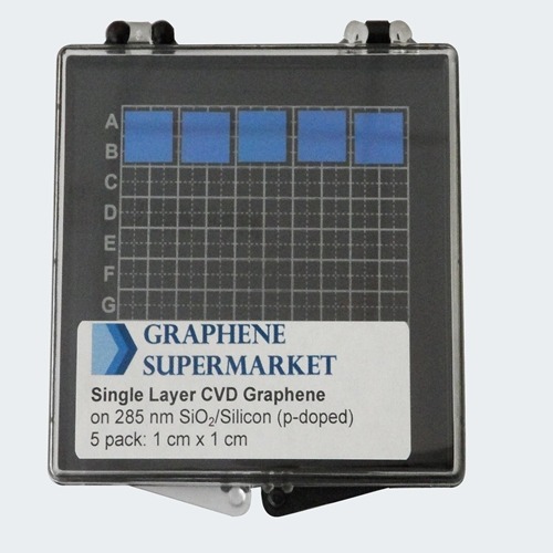
A five pack of monolayer graphene on 1cm x 1cm silicon wafers (p-doped) with a 285 nanometer silicon dioxide coating.Properties of Graphene Film:The thickness and quality of our graphene films is controlled by Raman Spectroscopy. The graphene coverage of this product is about 95% The graphene film is continuous, with occasional holes and cracks Organic and PMMA residues can be observed The graphene film is polycrystalline, i.e. it consists of grains with different crystallographic orientation Sheet Resistance: 660-1,500 Ω/square Raman Spectrum of Single-Layer Graphene on SiO2
Our graphene films are predominantly single-layer graphene (more than 90%) with occasional small multilayer islands (approximately 10%).Properties of Silicon/Silicon Dioxide Wafers:Oxide Thickness: 285 nm Color: Violet Wafer thickness: 525 micron Resistivity: 0.001-0.005 ohm-cm Type/Dopant: P/Boron Orientation: <100> Front Surface: Polished Back Surface: Etched RCA cleaned Applications:Graphene electronics and transistors Conductive coatings Aerospace industry applications Support for metallic catalysts Microactuators MEMS and NEMS Chemical and biosensors Multifunctional materials based on graphene Graphene Research Our graphene films are manufactured using a PMMA assisted transfer method. Please refer to the references below for more details. Optical Image of Single-Layer Graphene
![]()
Academic References / Read MoreGraphene Growth Large-Area Synthesis of High-Quality and Uniform Graphene Films on Copper Foils Science 5 June 2009: Vol. 324. no. 5932, pp. 1312 - 1314 Graphene Transfer Transfer of Large-Area Graphene Films for High-Performance Transparent Conductive Electrodes, Li et.al., Nano Lett., 2009, 9 (12), pp 4359–4363 Toward Clean and Crackless Transfer of Graphene Liang et.al.,ACS Nano, 2011, 5 (11), pp 9144–9153 |
Customers who bought this product also bought
|


 "19세 미만의 미성년자"는 출입을 금합니다!