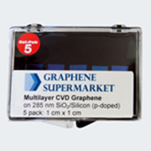
| 상품명 | Multilayer Graphene on 285 nm Silicon Dioxide Wafer: 5 pack |
|---|---|
| 상품요약정보 | A 5 pack of multilayer CVD-grown graphene transferred onto 1cm x 1cm silicon wafers (p-doped) with a 285 nanometer silicon dioxide coating. |
| 국내·해외배송 | 국내배송 |
| 배송방법 | 택배 |
| 배송비 | 2,500원 (50,000원 이상 구매 시 무료) |
| SNS 상품홍보 | |
|---|
배송주기

| 옵션선택 |
(최소주문수량 1개 이상 / 최대주문수량 0개 이하)
사이즈 가이드수량을 선택해주세요.
위 옵션선택 박스를 선택하시면 아래에 상품이 추가됩니다.
| 상품명 | 상품수 | 가격 |
|---|---|---|
| Multilayer Graphene on 285 nm Silicon Dioxide Wafer: 5 pack |


|
0 ( |
할인가가 적용된 최종 결제예정금액은 주문 시 확인할 수 있습니다.
The thickness and quality of our graphene films is controlled by Raman Spectroscopy
The graphene coverage of this product is about 95%
The graphene film is continuous, with occasional holes and cracks
The graphene film is polycrystalline, i.e. it consists of grains with different crystallographic orientation
Sheet Resistance: 660-1,500 Ω/square
The graphene grown on nickel film is multilayer and is not uniform. It looks like a patchwork whereas the “patches” have different thicknesses. The thickness of the film varies from 1 to 7 layers, with an average of 4. The graphene layers within the same patch are aligned relative to each other (there is a graphitic AB-staking order). The size of the patches is about 3-10 microns.
Properties of Silicon/Silicon Dioxide Wafers:
Oxide Thickness: 285 nm Color: Violet Wafer thickness: 525 micron Resistivity: 0.001-0.005 ohm-cm Type/Dopant: P/Boron Orientation: <100> Front Surface: Polished Back Surface: Etched
Applications:
Graphene electronics and transistors Conductive coatings Aerospace industry applications Support for metallic catalysts Microactuators MEMS and NEMS Chemical and biosensors Multifunctional materials based on graphene Graphene Research
Our graphene films are manufactured using a PMMA assisted transfer method. Please refer to the references below for more details.
Academic References / Read More
Graphene Growth Large-Area Synthesis of High-Quality and Uniform Graphene Films on Copper Foils Science 5 June 2009: Vol. 324. no. 5932, pp. 1312 - 1314 Graphene Transfer Transfer of Large-Area Graphene Films for High-Performance Transparent Conductive Electrodes, Li et.al., Nano Lett., 2009, 9 (12), pp 4359–4363 Toward Clean and Crackless Transfer of Graphene Liang et.al.,ACS Nano, 2011, 5 (11), pp 9144–9153 |
| SKU | MULTI-SIO2-5P | |
상품의 사용후기를 적어주세요.
게시물이 없습니다
상품에 대해 궁금한 점을 해결해 드립니다.
글읽기 권한이 없습니다.
 "19세 미만의 미성년자"는 출입을 금합니다!
| 번호 | 카테고리 | 제목 | 작성자 | 작성일 | 조회 |
|---|---|---|---|---|---|
| 2 |  견적 문의 드립니다. 견적 문의 드립니다.
|
양**** | 2024-03-18 | 2 | |
| 1 |  견적 문의 드립니다. 견적 문의 드립니다.
|
유니나노텍(주) | 2024-03-19 | 2 |


법인명(상호) : 유니나노텍(주) 대표자(성명) : 유니나노텍(주) 사업자 등록번호 안내 : [1428150860] 통신판매업 신고 2021-용인기흥-0779 [사업자정보확인]
전화 : 031-546-8733 팩스 : 주소 : 17015 경기도 용인시 기흥구 동백중앙로16번길 16-4 (중동) 에이스동백타워 1동 303호
개인정보보호책임자 : 유니나노텍(주)(nano@uninanotech.com)
Contact for more information.
Copyright © 유니나노텍(주). All rights reserved. hosting by cafe24 카페24(주)