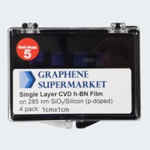
Single Layer CVD hexagonal Boron Nitride Film on 285 nm SiO2/Si substrates (p-doped), 1cmx1cm: 4 pack Properties of BN film 97% coverage with minor holes and organic residues High Crystalline Quality The Raman spectrum should peak at ~1369cm-1
![]()
The Raman Signal of BN on SiO2/Si is very weak. To characterize h-BN on SiO2/Si using Raman spectroscopy, you need to use a blue or high power laser and the signal may not be detectable on certain commercial systems. For more information regarding Raman spectroscopy and characterization of h-BN on SiO2/Si, refer to the following paper: Hunting for Monolayer Boron Nitride: Optical and Raman Signatures . The h-BN film is grown via CVD onto copper foil, then transferred to the SiO2/Si substrate. To see characterizations of the film before transfer, see our related product, h-BN on Copper Foil. Applications:BN on SiO2/Si wafers are ideal for creating graphene/BN interfaces, allowing the graphene to be precisely gated, increasing mobility, and reducing scattering. h-BN is appealing as a substrate for graphene-based electronics because its surface is atomically smooth, it is free of dangling bonds, and has an analogous structure to graphene. Using our h-BN on SiO2/Si wafers in conjunction with graphene, we encourage you to explore graphene heterostructures for transistor applications. We can offer custom sizes of hBN film on a 4" wafer. Please contact us at info@graphenelab.com for more details.
| SKU | 1ML-BN-SIO2-4P | | Weight | 0.10 lbs |
Detailed images
Customers who bought this product also bought
|


 "19세 미만의 미성년자"는 출입을 금합니다!