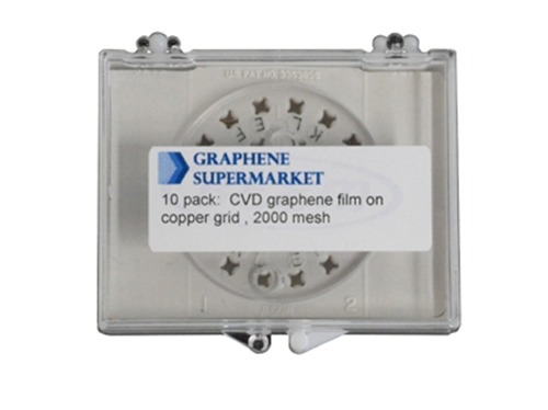
Trial pack: 10 CVD Graphene TEM grids includes: 5 CVD Graphene film deposited on lacey carbon TEM grids (300 Mesh) and 5 CVD Graphene film deposited on Copper TEM grids (2000 Mesh). Availability: In StockWe use CVD graphene grown on Ni to prepare TEM grids Thickness of CVD Graphene film: 0.3-2 nm (1-6 monolayers)Typical graphene coverage:60-90% Ultrathin CVD Graphene grids provide the ideal specimen support to achieve high resolution data in TEM imaging making them an ideal choice many TEM applications such as:CVD Graphene grids can be used for the applications: • Imaging of nanoparticles, proteins, viruses, DNA • Medical Diagnostics • Single Cell Studies • 3D protein imaging • Drug design • Imaging of Biological Markers and bio-inspired nanomaterials • Cryo-transmission electron microscopy, Electron Cryomicroscopy • Single Particle Analysis ( SPA ) • Materials science and Semiconductor Research • Electron Energy Loss Spectroscopy (EELS)
![]()
| | | SKU | SKU-TEM-CLC-10TP | | Weight | 0.10 lbs |
Customers who bought this product also bought- High Purity Micronized Graphite, 15 µm, 99%, 1kg
- Ultra Highly Concentrated Single-Layer Graphene Oxide, 500 ml
- Graphene-Silver Nanowires on PET, Size: 4cm x 4cm
- MoS2 Ultrafine Powder - 5 grams
- High Purity Micronized Graphite, 45 µm, 99%, 1kg
- Amorphous Graphite - 100 Grams
- Conductive Graphene Sheets, 8"x8", 10 pack
- Micronized Graphite, 25 µm, 96%, 250g
- FLEXIBLE SILVER/CARBON CONDUCTIVE EPOXY G6E-FXNS
- WS2 Micropowder - 100 grams
|