| 상품명 | Tungsten Ditelluride (WTe₂) |
|---|---|
| 상품요약정보 | Tungsten Ditelluride (WTe₂) |
| 국내·해외배송 | 국내배송 |
| 배송방법 | 택배 |
| 배송비 | 2,500원 (50,000원 이상 구매 시 무료) |
| SNS 상품홍보 | |
|---|
배송주기

| 옵션선택 |
(최소주문수량 1개 이상 / 최대주문수량 0개 이하)
사이즈 가이드수량을 선택해주세요.
위 옵션선택 박스를 선택하시면 아래에 상품이 추가됩니다.
| 상품명 | 상품수 | 가격 |
|---|---|---|
| Tungsten Ditelluride (WTe₂) |


|
0 ( |
할인가가 적용된 최종 결제예정금액은 주문 시 확인할 수 있습니다.
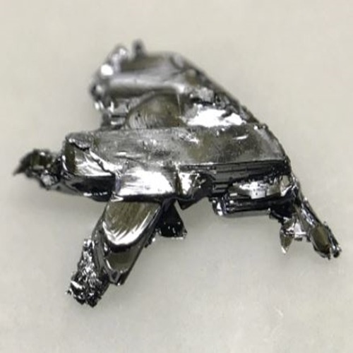
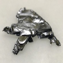
Typical characteristics of WTe2 crystals from 2Dsemiconductors USA
Growth method matters> Flux zone or CVT growth method? Contamination of halides and point defects in layered crystals are well known cause for their reduced electronic mobility, reduced anisotropic response, poor e-h recombination, low-PL emission, and lower optical absorption. Flux zone technique is a halide free technique used for synthesizing truly semiconductor grade vdW crystals. This method distinguishes itself from chemical vapor transport (CVT) technique in the following regard: CVT is a quick (~2 weeks) growth method but exhibits poor crystalline quality and the defect concentration reaches to 1E11 to 1E12 cm-2 range. In contrast, flux method takes long (~3 months) growth time, but ensures slow crystallization for perfect atomic structuring, and impurity free crystal growth with defect concentration as low as 1E9 - 1E10 cm-2. During check out just state which type of growth process is preferred. Unless otherwise stated, 2Dsemiconductors ships Flux zone crystals as a default choice.
XRD data collected from WTe2 crystals (sharpest XRD peaks in the commercial market)
Raman spectrum collected from WTe2 crystals (also sharpest and most defined Raman signal from commercial WTe2 crystals)
EDS spectrum collected from WTe2 crystals
Partial List of Published Articles Using Our WTe2 Crystals (as of 2017)
L. A. Walsh et. al. "WTe2 thin films grown by beam-interrupted molecular beam epitaxy" 2Dmaterials, 4, 2 (2017)
P. Lu et.al. Origin of superconductivity in the Weyl semimetal WTe2 under pressure, Phys. Rev. B. 94, 224512 (2016)
M. Kim et. al. Determination of the thickness and orientation of few-layer tungsten ditelluride using polarized Raman spectroscopy, 2D Materials, Volume 3, Number 3
Y. Kim. et.al. Anomalous Raman scattering and lattice dynamics in mono- and few-layer WTe2, Nanoscale, 2016,8, 2309-2316
상품의 사용후기를 적어주세요.
게시물이 없습니다
상품에 대해 궁금한 점을 해결해 드립니다.
게시물이 없습니다


법인명(상호) : 유니나노텍(주) 대표자(성명) : 유니나노텍(주) 사업자 등록번호 안내 : [1428150860] 통신판매업 신고 2021-용인기흥-0779 [사업자정보확인]
전화 : 031-546-8733 팩스 : 주소 : 17015 경기도 용인시 기흥구 동백중앙로16번길 16-4 (중동) 에이스동백타워 1동 303호
개인정보보호책임자 : 유니나노텍(주)(nano@uninanotech.com)
Contact for more information.
Copyright © 유니나노텍(주). All rights reserved. hosting by cafe24 카페24(주)