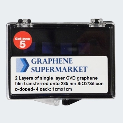
Properties of Silicon/Silicon Dioxide Wafers:Oxide Thickness: 285 nm Color: Violet Wafer thickness: 525 micron Resistivity: 0.001-0.005 ohm-cm Type/Dopant: P/Boron Orientation: <100> Front Surface: Polished Back Surface: Etched Applications:Graphene electronics and transistors Conductive coatings Aerospace industry applications Support for metallic catalysts Microactuators MEMS and NEMS Chemical and biosensors Multifunctional materials based on graphene Graphene Research Our graphene films are manufactured using a PMMA assisted transfer method.Please refer to the references below for more details. Academic References / Read MoreGraphene Growth Large-Area Synthesis of High-Quality and Uniform Graphene Films on Copper Foils Science 5 June 2009: Vol. 324. no. 5932, pp. 1312 - 1314 Graphene Transfer Transfer of Large-Area Graphene Films for High-Performance Transparent Conductive Electrodes, Li et.al., Nano Lett., 2009, 9 (12), pp 4359–4363 Toward Clean and Crackless Transfer of Graphene Liang et.al.,ACS Nano, 2011, 5 (11), pp 9144–9153 | 


 "19세 미만의 미성년자"는 출입을 금합니다!