| 상품명 | Full area coverage CVD MoTe2 few-layers |
|---|---|
| 상품요약정보 | Full area coverage CVD MoTe2 few-layers |
| 국내·해외배송 | 국내배송 |
| 배송방법 | 택배 |
| 배송비 | 2,500원 (50,000원 이상 구매 시 무료) |
| SNS 상품홍보 | |
|---|
배송주기

| 옵션선택 |
(최소주문수량 1개 이상 / 최대주문수량 0개 이하)
사이즈 가이드수량을 선택해주세요.
위 옵션선택 박스를 선택하시면 아래에 상품이 추가됩니다.
| 상품명 | 상품수 | 가격 |
|---|---|---|
| Full area coverage CVD MoTe2 few-layers |


|
0 ( |
할인가가 적용된 최종 결제예정금액은 주문 시 확인할 수 있습니다.
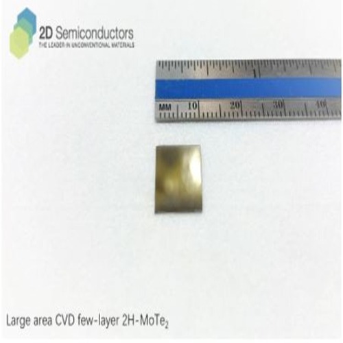
2H semiconducting phase few-layer MoTe2 (3-6 layers) has been grown on 1cm2 size c-cut sapphire substrates using low-pressure chemical vapor deposition technique (LPCVD). Grown sheets can also be transferred onto other substrates such as quartz, SiO2/Si, PET, metals, and others on request. Few-layer MoTe2 reach full area coverage on sapphire, exhibit outstanding environmental stability, surface smoothness, and uniformity. Grown sheets are environmentally stable and exhibit band gap between bulk (0.6 eV) and monolayer (1.1 eV).
Special note: Despite extensive R&D efforts, CVD grown monolayer MoTe2 are environmentally rather unstable due to uncontrollable defect characteristics. We are unable to provide monolayer thick MoTe2 at this time.
Growth method: Our company synthesizes these few layers using chemical vapor deposition (CVD) using highest purity (6N) gases and precursors in semiconductor grade facilities to produce crystalline and large domain size samples (1-50um). Other sources typically use MOCVD or sputtering process wherein defects are very large, domain sizes are small (10nm-500nm), and products are non-layered. Our samples are always highly crystallized, high purity, and perfectly layered.
Characteristics of CVD grown 2H (semiconducting phase) MoTe2 sheets by 2Dsemiconductors Inc.
| Sample size | 1cm x 1cm square shaped |
| Substrate type | c-cut sapphire (default) other substrates on demand |
| Coverage | Full-area coverage |
| Electrical properties | 0.8-1.0 eV semiconductor |
| Crystal structure | Hexagonal Phase |
| Unit cell parameters | a = b = 0.350 nm, c = 1.341 nm, α = β = 90, γ = 120° |
| Production method | Low pressure Chemical Vapor Deposition (LPCVD) |
| Characterization methods | Raman, photoluminescence, TEM, EDS |
상품의 사용후기를 적어주세요.
게시물이 없습니다
상품에 대해 궁금한 점을 해결해 드립니다.
글읽기 권한이 없습니다.
 "19세 미만의 미성년자"는 출입을 금합니다!
| 번호 | 카테고리 | 제목 | 작성자 | 작성일 | 조회 |
|---|---|---|---|---|---|
| 1 |   상품 견적 문의 드립니다. 상품 견적 문의 드립니다.
|
유니나노텍(주) | 2022-02-10 | 0 |


법인명(상호) : 유니나노텍(주) 대표자(성명) : 유니나노텍(주) 사업자 등록번호 안내 : [1428150860] 통신판매업 신고 2021-용인기흥-0779 [사업자정보확인]
전화 : 031-546-8733 팩스 : 주소 : 17015 경기도 용인시 기흥구 동백중앙로16번길 16-4 (중동) 에이스동백타워 1동 303호
개인정보보호책임자 : 유니나노텍(주)(nano@uninanotech.com)
Contact for more information.
Copyright © 유니나노텍(주). All rights reserved. hosting by cafe24 카페24(주)