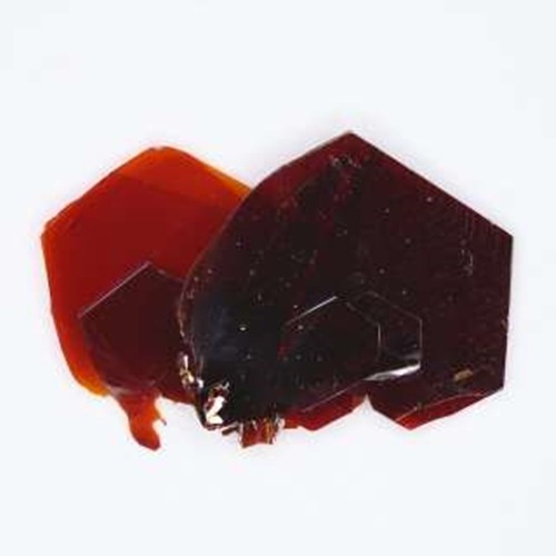
| 상품명 | HfS2 (Hafnium Disulfide) |
|---|---|
| 상품요약정보 | HfS2 (Hafnium Disulfide) |
| 국내·해외배송 | 국내배송 |
| 배송방법 | 택배 |
| 배송비 | 2,500원 (50,000원 이상 구매 시 무료) |
| SNS 상품홍보 | |
|---|
배송주기

| 옵션선택 |
(최소주문수량 1개 이상 / 최대주문수량 0개 이하)
사이즈 가이드수량을 선택해주세요.
위 옵션선택 박스를 선택하시면 아래에 상품이 추가됩니다.
| 상품명 | 상품수 | 가격 |
|---|---|---|
| HfS2 (Hafnium Disulfide) |


|
0 ( |
할인가가 적용된 최종 결제예정금액은 주문 시 확인할 수 있습니다.
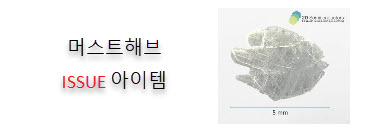
| Crystal size | ~10 mm |
| Electrical properties | Semiconductor |
| Crystal structure | Hexagonal |
| Unit cell parameters | a = b = 0.363 nm, c = 0.586 nm, α = β = 90°, γ = 120° |
| Type | Synthetic |
| Purity | >99.995 % |
| Characterized by | XRD, Raman, EDX |
| More information? | Please contact us by email or phone |
XRD: single crystal and powder X-ray diffraction (D8 Venture Bruker and D8 Advance Bruker)
EDX: Energy-dispersive X-ray spectroscopy for stoichiometric analysis
Raman: 785nm Raman system
Click on an image to zoom
X-ray diffraction on a HfS2 single crystal aligned along the (001) plane. XRD was performed at room temperature using a D8 Venture Bruker. The 4 XRD peaks correspond, from left to right, to (00l) with l = 1, 2, 3, 4
Powder X-ray diffraction (XRD) of a single crystal HfS2. X-ray diffraction was performed at room temperature using a D8 Venture Bruker.
Raman spectrum of a single crystal HfS2. Measurement was performed with a 785 nm Raman system at room temperature.
1. Toru Kanazawa et al., "Few-layer HfS2 transistors", Sci. Rep. 2016, 6: 22277 (2016), link to article:http://www.ncbi.nlm.nih.gov/pmc/articles/PMC4772098/
2. Kai Xu et al., "Ultrasensitive Phototransistors Based on Few-Layered HfS2", Adv. Mat. 27, 7881-7887 (2015), link to article:hhttp://onlinelibrary.wiley.com/doi/10.1002/adma.201503864/full
상품의 사용후기를 적어주세요.
게시물이 없습니다
상품에 대해 궁금한 점을 해결해 드립니다.
글읽기 권한이 없습니다.
 "19세 미만의 미성년자"는 출입을 금합니다!
| 번호 | 카테고리 | 제목 | 작성자 | 작성일 | 조회 |
|---|---|---|---|---|---|
| 4 |  견적문의드립니다. 견적문의드립니다.
|
김**** | 2024-03-05 | 2 | |
| 3 |  견적 문의드립니다 견적 문의드립니다
|
유니나노텍(주) | 2024-03-07 | 5 | |
| 2 | 견적 문의 드립니다
|
류**** | 2022-10-14 | 2 | |
| 1 | 다음 제품 견적 문의드립니다.
|
유니나노텍(주) | 2022-10-20 | 27 |


법인명(상호) : 유니나노텍(주) 대표자(성명) : 유니나노텍(주) 사업자 등록번호 안내 : [1428150860] 통신판매업 신고 2021-용인기흥-0779 [사업자정보확인]
전화 : 031-546-8733 팩스 : 주소 : 17015 경기도 용인시 기흥구 동백중앙로16번길 16-4 (중동) 에이스동백타워 1동 303호
개인정보보호책임자 : 유니나노텍(주)(nano@uninanotech.com)
Contact for more information.
Copyright © 유니나노텍(주). All rights reserved. hosting by cafe24 카페24(주)